Product
An AI toolkit that engineers circuit boards, from agreed inputs to a fab-ready KiCad release.
Product overview
ZeroErrata · AI toolkit for electronics design
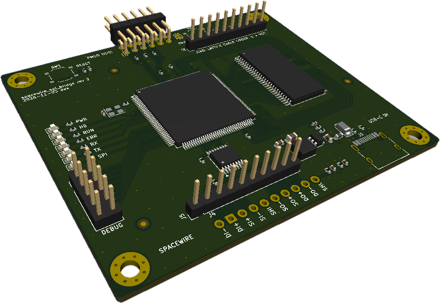
Requirements in.Fab-ready boards out.
A language model working through build scripts, linters, a field solver, thermal and RF models and a release pipeline. It takes a board from agreed inputs to a fab-ready KiCad release, with an engineer approving every checkpoint.
Zero DRC / Zero ERC / Zero Errata
FPGAMachXO2-7000HC · TQFP-144
Buffer32 MB SDRAM · 100 MHz
ImpedanceLVDS 100.0 Ω · SE 50.1 Ω
Test run 10 · draftSpaceWire to SPI bridge
Layers4, controlled impedance
Size78 × 66 mm
AssemblyPCBA both sides
ERC0
DRC0 / 0 / 0
01 — PlatformWhat the tool is
A board that passes DRC is not yet a good board. ZeroErrata is the engineering layer between a language model and a board you would sign off.
0 / 0 / 0
DRC violations, unconnected items and parity errors on every release
1:1
byte-for-byte rebuild of every released board from its scripts
9
release gates, from ERC to thermal margins, before a board ships
A / Basis
Built on open-source practice
The design rules come from a study of published open-source hardware by research labs and hardware companies. Each rule is tied to a check that measures it on the board.
B / Adaptation
Extended for your domain
Rules, reference designs, part preferences and review findings are plain project files. They can be extended with a team's own standards and past designs, so the system follows the conventions of a specific product line.
C / Toolkit
A toolkit, not a connector
Connecting a language model to KiCad gives it access to an editor. ZeroErrata gives it the engineering tools: build scripts, linters, a field solver, thermal and RF models, and a release pipeline.
D / Reproducibility
Every board is code
Placement, copper, pours and release are scripts, not hand edits. A fix is a change to a script and a re-run, and every result can be checked and rebuilt by an engineer.
02 — Live sessionNew · experimental
The AI drives the CAD. The gates decide.
Every step runs through a script or a check, so each action leaves a result that can be read, reviewed and rerun.
claudeinputs agreed: SpaceWire ⇄ SPI bridge, SDRAM FIFO, 4 layers
claudegen_sch.py → A2 sheet, 7 wired blocks
kicadERC ..................... 0 errors · 0 warnings
claudeproj_setup.py → classes SE50 · LVDS100 · Power · Ground
claudeplace.py → 98 parts from geo.py
clauderoute.py sdram_fan
clauderoute.py sdram_wraps
clauderoute.py lvds_pairs · spw · power_stubs
routerleftovers JTAG · config · reset · IRQ → frozen seed
claudepost.ps1 → pours, stitching, return vias
kicadDRC + parity ............ 0 / 0 / 0
lintpcb_lint ................ 0 FAIL · 0 WARN
lintrf_lint ................. SE 50.1 Ω · LVDS 100.0 Ω
reviewsecond opinion .......... all rules triaged
fpfootprints vs LCSC ...... CPL corrected
partssourcing ................ LCSC numbers on the BOM
modelthermal ................. 0.73 W · max 34.1 °C
renderreview tiles ............ no 90° bends
exportgerbers · drill · BOM · CPL · PDFs · report
RELEASE · READY FOR FAB
G1ERCwaitPASS
G2DRC + paritywaitPASS
G3pcb_lintwaitPASS
G4rf_lintwaitPASS
G52nd opinionwaitPASS
G6FootprintswaitPASS
G7SourcingwaitPASS
G8ThermalwaitPASS
G9VisualwaitPASS
Representative session, condensed from the build chain of test run 10, the SpaceWire bridge.
03 — EngineeringRouting
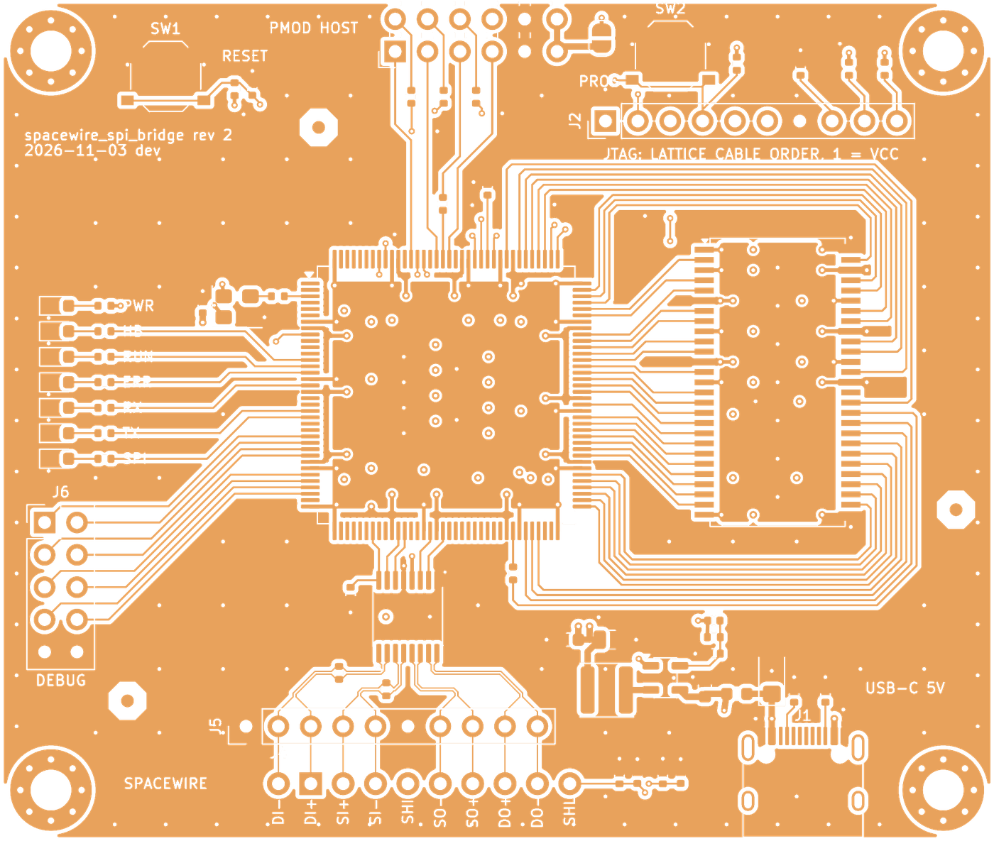
Routed the way an engineer would.
- 01Placement from one geometry fileEvery coordinate, pin map and net order of the board lives in a single module.
- 02The SDRAM bus as a 45° fanThe memory bus leaves the FPGA as one disciplined bundle, not a tangle.
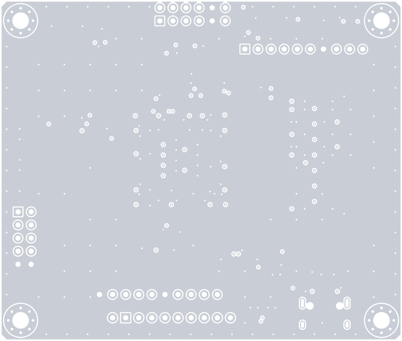
- 03Nested wraps around the memoryThe far row is carried around both ends of the package in parallel lanes.
- 04The router only for leftoversSlow nets go to the router under project rules; its result is frozen for reproducibility.
schematic · A2 · inverted
04 — SchematicNew · experimental
One sheet. Seven wired blocks.
The schematic is generated from the same geometry and pin maps as the layout, so the drawing and the copper cannot drift apart.
- 01Power input. USB-C 5 V, TVS, ferrite, TLV62569 buck to 3.3 V
- 02FPGA power. 100 nF at every VCC and VCCIO pin, 10 µF per bank
- 03Configuration. Internal flash, JTAG for the Lattice cable
- 04SDRAM FIFO. W9825G6KH, 32 MB at 100 MHz
- 05Host SPI. Slave to 80 MHz, IRQ, reset, Pmod 2A
- 06SpaceWire. SN65LVDS049, micro-D or lab header
- 07Clock and status. 25 MHz, reset, LEDs, debug header
05 — Stackup4 layers
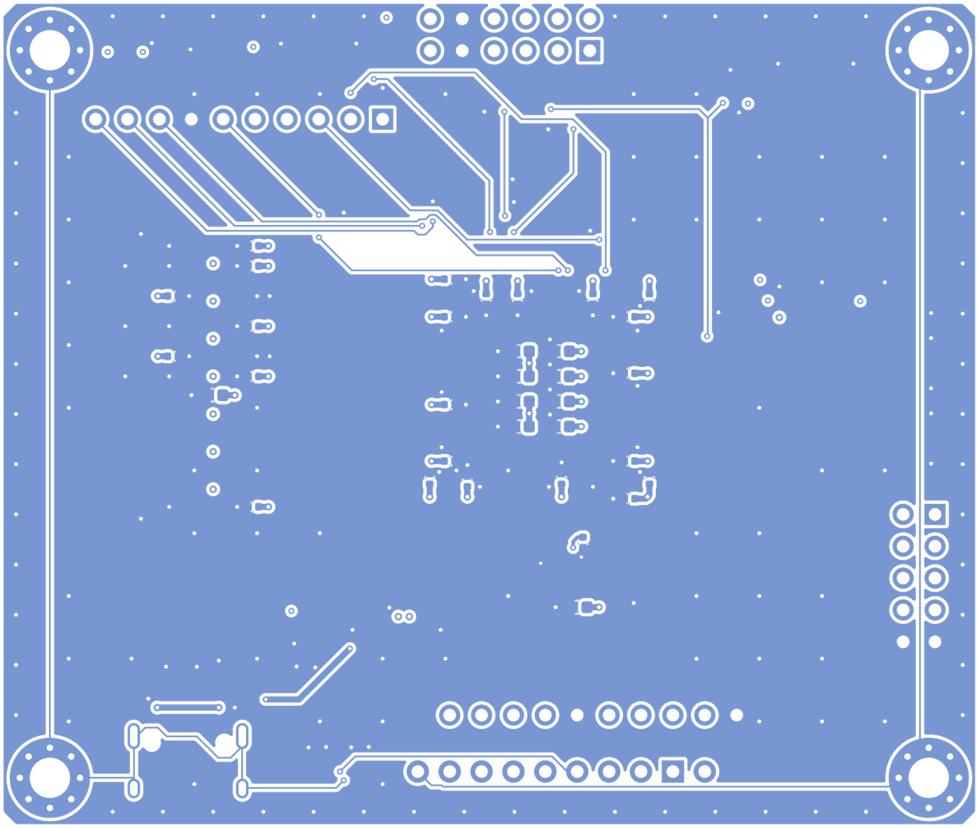
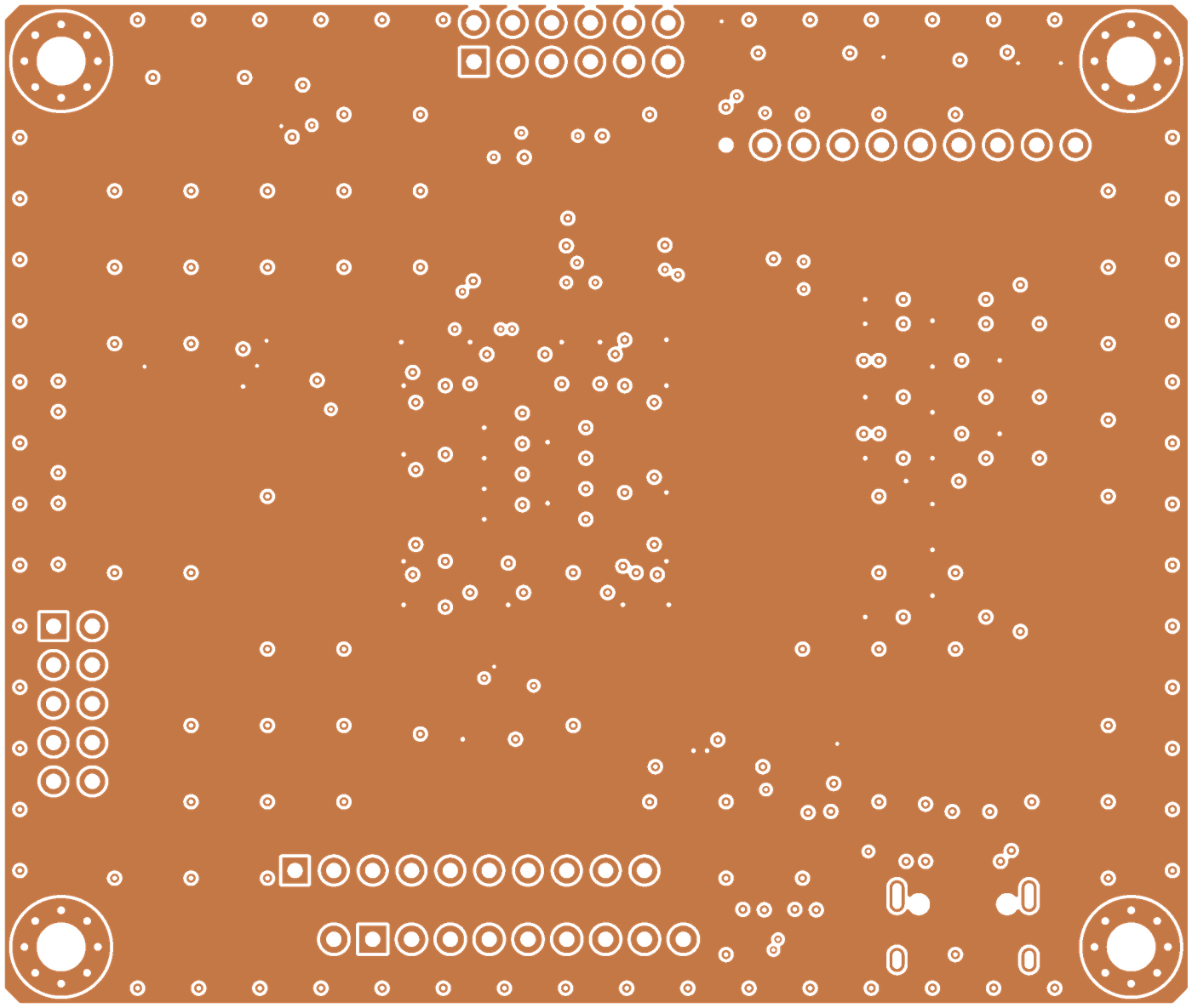
Four layers. One intent.
- F.Cu · signalFPGA fan-out, SDRAM bus, LVDS pairs into the SpaceWire rows.
- In1.Cu · groundAn unbroken reference plane under every fast line.
- In2.Cu · 3.3 VThe supply plane, with fills under both packages.
- B.Cu · decouplingA 100 nF capacitor directly under every FPGA and SDRAM supply pin.
06 — Process8 stages · 6 checkpoints
AI does the engineering. Engineers keep command.
Every board passes through fixed stages. Each checkpoint is approved before the next stage starts, and every decision is logged with its alternatives and the reason.
01
Inputs
Function, key parts with alternatives, rails and currents, outline, connectors, layers, fab and assembly.
■ Owner checkpoint02
Feasibility
Density patches under DRC, space budget, channel map and the power path.
■ Checkpoint, dense boards03
Schematic
Wired blocks with labels between them, ERC at zero, netlist and PDF.
■ Owner checkpoint04
Board setup
Net classes, custom design rules, stackup, outline and mounting.
□ Automatic05
Placement
Mechanics first, then the main ICs, support parts within 1 to 3 mm of their pins.
■ Owner checkpoint06
Routing
Power and critical nets first, buses as 45° bundles, ground stitching, leftovers last.
■ Owner checkpoint07
Checks
ERC, DRC with parity, linters, renders, an independent second opinion and physical models.
□ Part of routing review08
Release
Order package, design report, annotated version tag and an updated project state.
■ Owner checkpoint07 — VerificationRelease gates
A clean DRC is the entry condition. Not the result.
A board is released only when every gate passes. A failure cannot be waived. A warning is fixed, or accepted in writing with a reason that ships in the report.
#GateToolPass conditionState
G1SchematicKiCad ERC0 errors, 0 warningsPASS
G2BoardKiCad DRC + parity0 violations, 0 unconnected items, 0 parity errors, zones refilledPASS
G3Layout craftpcb_lintBend angles, width changes, via sizes, return vias, stitching, decoupling distance, silkscreen, BOM coveragePASS
G4RF and fast linesrf_lintImpedance, skew, return vias, reference planes and stubs within limitsPASS
G5Independent reviewsecond opinionAn independent analyzer suite; every error and warning rule triagedPASS
G6Assembly datafootprint checkLand patterns compared with supplier footprints, placement rotations correctedPASS
G7Parts and pinssourcing + pincheckParts in stock with order numbers; MCU pins match the datasheet tablesPASS
G8Physical modelsthermal · S-param · SPICEJunction temperatures and margins stated in the design reportPASS
G9Visual reviewrenders + tilesNo 90° bends, no autorouter look, support parts at their pinsPASS
08 — Cross-checkNew · experimental
A script does not read O as 0.
Net labels, pin tables, part numbers and datasheet values are compared character by character and number by number. Lookalike glyphs and a misplaced decimal point are caught where the eye skims past.
#ReferenceAs drawnResult
01SD_DQ10SD_DQ1Ocol 7 · U+004F ≠ U+0030
02SPW_DIN_PSPW_DlN_Pcol 6 · U+006C ≠ U+0049
03LVDS_DOUT_NLVDS_DOUT_Nmatch
04SD_BA1SD_BAlcol 6 · U+006C ≠ U+0031
05SD_WE_NSD_VVE_Ncol 4 · V+V ≠ U+0057
06SPW_SOUT_PSPW_5OUT_Pcol 5 · U+0035 ≠ U+0053
07PROGRAMNPROGRAMNmatch
08R3 453k → 3.32 VR3 45.3k → 0.87 VVOUT off by 3.8×
O≠0
U+004F
Latin capital OU+0030
Digit zero
Latin capital OU+0030
Digit zero
I≠l
U+0049
Latin capital IU+006C
Latin small l
Latin capital IU+006C
Latin small l
1≠l
U+0031
Digit oneU+006C
Latin small l
Digit oneU+006C
Latin small l
VV≠W
U+0056 ×2
Two capital VU+0057
Latin capital W
Two capital VU+0057
Latin capital W
5≠S
U+0035
Digit fiveU+0053
Latin capital S
Digit fiveU+0053
Latin capital S
B≠8
U+0042
Latin capital BU+0038
Digit eight
Latin capital BU+0038
Digit eight
rn≠m
U+0072 U+006E
r followed by nU+006D
Latin small m
r followed by nU+006D
Latin small m
- PinsMCU pin maps against the datasheet tables
- FootprintsLand patterns against supplier footprints
- PartsMPN and order numbers against stock
- NetsSchematic netlist against board copper
09 — PhysicsThermal model
Every release knows its temperature.
A steady-state thermal model of the routed board, from part dissipation and track currents. Junction temperatures and margins go straight into the design report.
Model output from the release package. Bench measurement of the first articles is the next milestone.
Field solverMicrostrip, CPWG, stripline and differential pairs on the real stackup.
S-parametersRF chains cascaded with gain, match, noise figure and stability.
SPICE benchesAnalog nodes simulated with datasheet limits as pass checks.
openEMS3D models of antennas and filters with Smith charts.
10 — SourcingNew · experimental
Every line sourced before the order.
Manufacturer part numbers, supplier order numbers and stock are checked by the build chain, and the land patterns are compared with the supplier's own footprints.
35
BOM lines, SpaceWire bridge
93
parts in the BOM
34 / 35
lines with LCSC numbers
CPL
rotations checked against LCSC
11 — Test runsAll test runs →
Made by ZeroErrata — test runs.
Boards the tool produced during development, from FPGA to RF to power. They are drafts run end to end to test the system, not products for sale. Full sheets with specifications and verification results are in Test runs.
12 — DeliverablesRelease package
Every release ships complete.
Not a layout file and a promise. The full package a fab, an assembler and a reviewer need, written by the build chain and tagged in version control.
- 01Order packageGerber and drill archive, BOM and pick-and-place in KiCad and JLCPCB formats
- 02Design reportParts and the reasons for them, current rating, grounding, results, accepted warnings, first-article checklist
- 03DrawingsSchematic and board-layer PDFs, 3D renders, assembly sheets
- 04Verification recordERC and DRC reports, linter reports, second-opinion triage, footprint check
- 05AnalysesThermal maps, RF cascades, SPICE benches, EM models where the board needs them
- 06Decision logEvery choice with its alternatives and the reason, kept for the life of the design
# rebuild every released board from a clean state
> scripts\test.ps1

  tool tests ........................ pass
  rebuild released boards ........... done
  copper, footprints, zones ......... match
  outline and texts ................. match
  lint counts ....................... match
  JLCPCB placement data ............. match

SELF-TEST PASSED
13 — QuestionsNew · experimental
What engineering leads ask first.
Short answers on tools, ownership and where the work stands today.
Q1 / Tools
Which EDA does it use?
KiCad 10, with native project files. Every design opens in KiCad like any other project, with no proprietary format in between.
Q2 / People
What does the engineer still do?
Sets the inputs, approves the schematic, placement, routing and release, and decides every open point. The AI does the engineering work between checkpoints.
Q3 / Standards
Can it follow our design rules?
Rules, checks, templates and part preferences are plain files in the repository. A team's own standards and reference designs are added the same way.
Q4 / Files
Where do the design files live?
In a Git repository, with every stage, decision and release tag. Each board rebuilds from its scripts, so a reviewer can reproduce any result.
Q5 / Status
Has a board been manufactured?
Not yet. Designs are verified by checks, models and simulation. Manufacturing and bench measurement of the first articles is the next step.
Q6 / Fab
Which manufacturers are supported?
Order packages are written in KiCad and JLCPCB formats. Gerber, drill, BOM and placement files work with any board house and assembler.
14 — Briefing
Bring a requirement. Leave with a board.
We walk your team through a live design, from the first prompt to the order package, on a board from your own domain.